


The demand for more and more sophisticated electronics with steadily increasing data rates and performance in today’s cars and trucks, combined with the harsh conditions that automotive Ethernet interfaces operate in, makes it more and more challenging to design reliably. A top-down analysis methodology is a good strategy to design these interfaces efficiently. Cadence presents the results in an in-depth study.
The explosion of in-car electronic content in today’s automobiles is quickly changing the tools and methodologies needed to successfully deliver high-performance, reliable functionality to the automotive consumer. Automotive printed circuit board (PCB) design has traditionally consisted of interconnecting a few simple components, using two-layer PCBs, with the main concern being cost. But with the proliferation of advanced driver assistance systems (ADAS), cars can now contain as many as 100 electronic control modules (ECUs) connected to sensors located around the car through multiple yards of cable harnesses.
The signaling between the components used in cars is also changing in order to accommodate higher performance transmission between sensors, digital logic, and ECUs. The current standard being designed into most cars today is 100BASE-T1, which consists of 100Mbps operation over a single, balanced, twisted-pair cable, using PAM3 signaling in a very noisy automotive environment. And future designs are utilizing 1000BASE-T1, at 10X the data rate. This has significant implications on the associated system-level analysis required to ensure reliable operation. As we have seen in the computing, telecom, and mobile segments previously, as signaling moves to higher data rates, things that were safely overlooked in the past start to matter. Signal integrity (SI) effects like reflections, crosstalk, interconnect losses, and equalization all become important. New tools and methodologies are required to successfully design these complex interfaces on schedule.
A top-down analysis approach can be utilized to help make the overall design methodology more efficient. Starting in the earliest stages of the design cycle, a “virtual prototype” of the automotive Ethernet interface can be built, using estimated chip, package, board, connector, and cable models. This enables simulations to be run, and initial analyses to be performed to examine feasibility and design tradeoffs. For example, different lengths and types of cables can be simulated with different receiver equalization capability, to assess the impact on the eye diagrams at the receiver, and the bit error rate (BER) of the automotive Ethernet link.
As the design process marches forward, estimated models can be replaced with more detailed, design-specific models, making the analysis more accurate throughout the design cycle. Extraction tools can be used to extract S-parameters for package and PCB interconnect parasitics, which can be combined with connector and cable models from suppliers and lab measurements to enable end-to-end system simulation. IBIS-AMI models can be used to represent SerDes equalization functionality such as continuous time linear equalization (CTLE) and decision feedback equalization (DFE), enabling PAM3 signals to be compared and reviewed for different scenarios.
Automated compliance kits for automotive Ethernet can be leveraged to automatically analyze critical criteria per the associated interface standard, such as insertion and return losses, as well as the BER for the overall link. This capability can be deployed at the early “virtual prototype” stage, all the way through the design process to eventually perform final verification of your design before releasing to manufacturing.
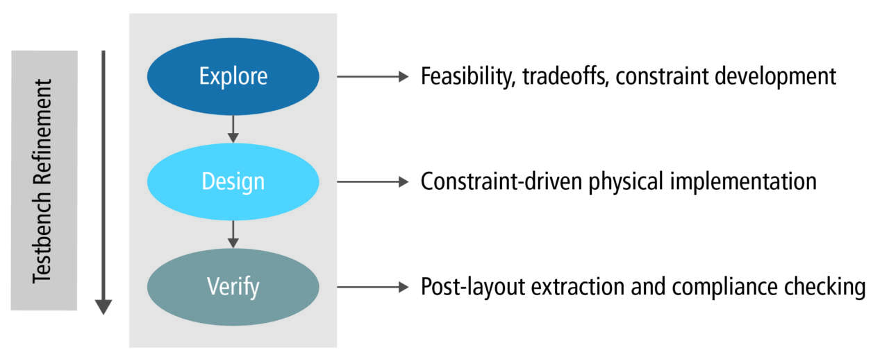
Top-Down SI Design Methodology
One key element to a successful methodology for interfaces at these data rates is to move the starting point significantly upstream of the traditional post-layout verification step. There is a false notion that, in a traditional “bottoms-up” methodology, meaningful analysis cannot be performed until after detailed PCB layout is done. Reality in a hardware design environment is quite different.
In order to accomplish a confident signoff for your critical interface in the compressed back-end of this PCB design process, preparation is critical. One strategy is to go “top down” and build an early version of a simulation testbench of your serial link interface, well in advance of that late stage. This can start upstream of detailed schematic capture, at the early bill of materials (BOM) stage, when you get an initial understanding of the SerDes and protocol that will be used to transmit and receive signals, a general idea of the partitioning of the system, the anticipated PCB stack-up and signal lengths, and what connectors and cables will likely be used. Detailed models for all the blocks in the system are not critical at this early stage, and “placeholders” can be used, with the understanding that they will be replaced later as more detail becomes available. (Compliance kits are a rich source of preliminary models for your early testbench and will be covered later in this article.) In a nutshell, if you can draw the interface on a napkin, you should be able to put together an early simulation testbench. The benefits to this kind of top-down methodology are multiple:
- it makes you visualize the overall system, and the signal path that will be traversed;
- it helps you identify all the models you will need to complete the overall die-to-die signal path, so you can work on obtaining them before you need them.
- getting something running early on makes you get your simulation testbenches set up ahead of time, so that subsequent runs throughout the process are largely a matter of updating models in the topology and re-running simulations in greater detail. This is a big time-saver at the back-end of the process, when time is short.
General design methodology
With an initial prototype of your interface topology in place, and at least placeholder models assigned to the various blocks, you should have a testbench that simulates and passes traffic at the targeted data rate. Now the work begins to replace models with more detailed, more realistic models as you go through the design process. These models generally fall into one of several general categories:
- IBIS-AMI models for SerDes transmitters and receivers;
- Spice models for discretes (ex. AC coupling caps);
- Packages;
- PCBs;
- Connectors.
The first step is to do a gap analysis between the models you need for the various blocks in the topology, and the models you have on hand in your library. Augment your testbench with the models that you have and verify that they simulate cleanly. Next, make list of the models that are missing, contact the model supplier (which can be internal or external), and put in requests for the models that you need. Keep track of who you had contact with, the dates of contact, and the status of the model. As you get them, augment your testbench accordingly. (Fig. 1)
Creating a Virtual Prototype
As one might expect, the easiest way to create a virtual prototype of your interface is to start with a pre-existing one from a previous project and modify it from there. Previous projects can be stored and re-used as “templates” to leverage as the starting point for your next one. In absence of that, a good starting point can be from a compliance kit from your EDA tool. An example 100BASE-T1 compliance kit topology is shown in Fig. 2.

This topology is derived from the 100BASE-T1 specification and represents the entire die-to-die signal path. This includes spec-level driver and receiver models, and example package, PCB, connector, and cable models. Also included is a spec-level IBIS-AMI model that represents equalization in the receiver. This can include functionality such as CTLE and DFE.
The topology shown above is essentially “graphical SPICE”. Standard modeling formats like IBIS, Touchstone, and SPICE subcircuits can all be assigned to blocks in the topology. The template above contains example models for five sections of 3m-long cable, which represents the longest length defined in the 100BASE-T1 specification. These model sections (and associated connectors) can easily be turned on and off to represent the lengths expected for your project.
While compliance kits can be leveraged to help build the initial virtual prototype of your interface, with working example models provided for all the blocks, this is just a starting point. All of these initial models should eventually be replaced by specific models with data from your actual project. (Fig. 3)
Building and Using IBIS-AMI Models for Receiver Equalization
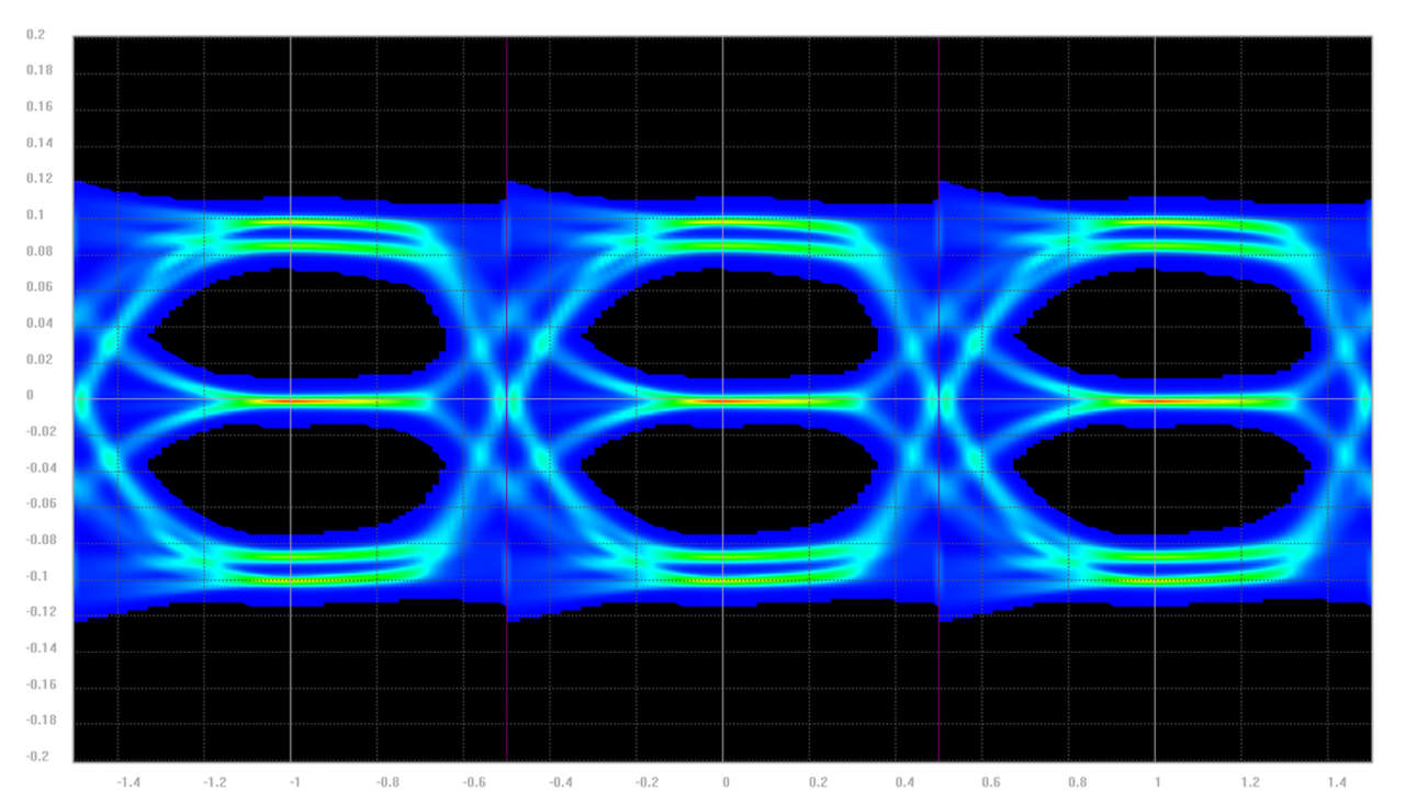
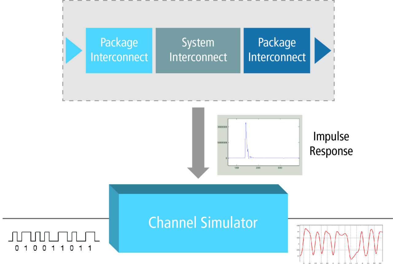
One of the key requirements for automotive applications such as automotive Ethernet is to meet a specific BER, for example 1e-10 for 100BASE-T1 interfaces. This is well beyond the scope of traditional circuit simulation and pushes into the channel simulation space used for popular serial link interfaces like PCI Express and USB. Circuit simulation is used to characterize the channel as an impulse response, which is then passed to the channel simulator, where it is convolved with a large bitstream stimulus to produce waveforms at the receiver, as shown in the Fig. 4.
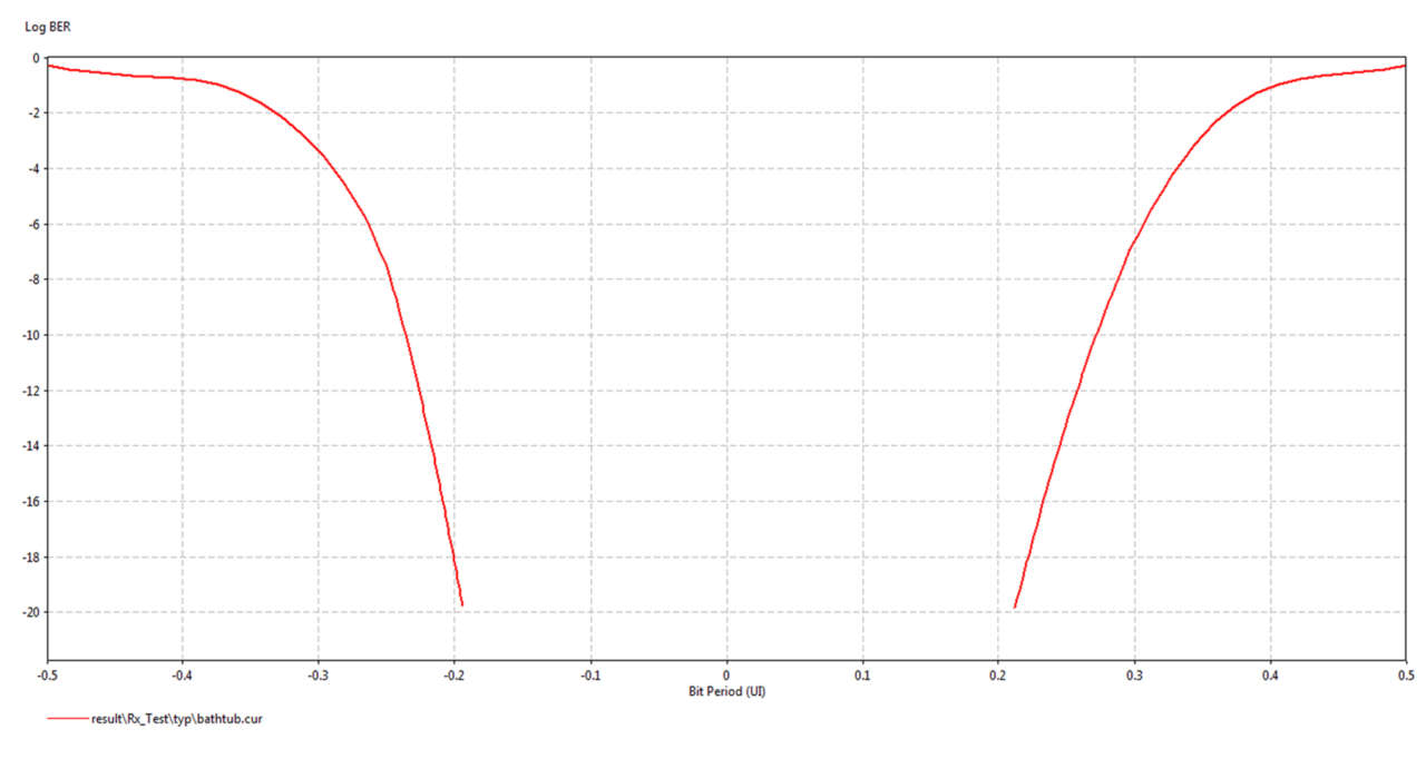
Channel simulation has the capacity to simulate tens of millions of bits of traffic in a reasonable time, enabling detailed eye distributions to be produced. These eye distributions are post-processed to produce bathtub curves that predict eye width and height at a particular BER. (Fig. 5)
To represent equalization in transmitters and receivers during channel simulation, IBIS-AMI models are used. As channel simulation techniques are still relatively new in the automotive space, it may sometimes be necessary for the SI engineer to build their own AMI models, based on data sheet specifications and knowledge about the SerDes devices being used in the interface.
IBIS-AMI models today can be quickly generated with EDA tools, taking input data such as the number of DFE taps, the limits on those taps, and the characteristics of the CTLE, if present. CTLE functionality can be modeled in a variety of text-based formats, such as step responses in the time domain, real/imaginary, magnitude/phase, or magnitude plots in the frequency domain, or as pole zero or rational functions.
Electromagnetic Emissions (EMC): One of the Biggest Problems in the Automotive Industry
For quite a few applications, the need to analyze electromagnetic emissions (EMC analysis) quickly becomes a complex and hard-to-control problem due to the three-dimensional nature of the design. Cadence Sigrity PowerSI technology allows the analysis of emissions as a post-process according to a signal and power integrity simulation. The developer concentrates on exactly the emissions that originate from the PCB and the substrate (IC package), whereby PCBs, supplies—especially their edge areas and recesses (voids)—and wire bonds are given special attention. In addition, the power/ground loop impedance is calculated as frequency-dependent, with all decoupling capacitors being extracted at the PCB or IC package level and included in the calculation.
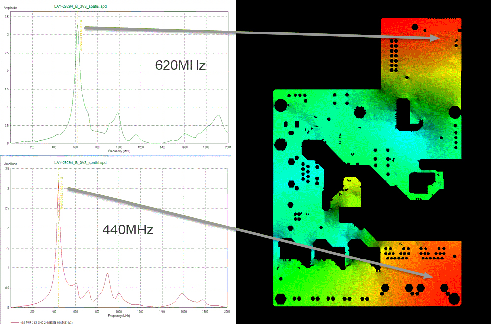
An impedance profile created this way provides excellent information about the frequency range and extent of the expected emissions by means of the calculated resonance frequencies and impedances. Also, an impedance profile is a suitable tool to find a problem-solving approach: suitable decoupling capacitors can attenuate the resonances and shift them to another, more harmless frequency band away from the high-energy clock frequency and its harmonic harmonics. (Fig. 6) Such an optimized supply system greatly maximizes the likelihood of successfully passing all EMC testing on the first attempt.
Standards-Based Compliance Analysis
With detailed interconnect models in place for your project, and IBIS-AMI models assigned and executing, compliance checking can be automatically performed against the automotive Ethernet standard you are designing to.
Each interface has some of its own specific criteria to be met. In this case, the 100BASE-T1 specification identifies a number of frequency domain criteria for the passive interconnect channel, as well as eye height and width criteria at a BER of 1e-10.
It can be very time-consuming to evaluate each of these criteria individually, especially if multiple runs are required to sweep corners and multiple channel models. Automated compliance kits can dramatically speed up your compliance checking and accelerate your time to signoff.
Automated sweeping of critical parameters and flagging of compliance failures enables better coverage of your automotive Ethernet interface design and helps to pinpoint any remaining areas of concern.


