


Miniaturization has made it more difficult to align multiple connectors, but design best practices and early engagement with a connector provider can help ensure design success.
Manufacturers of printed circuit boards (PCBs) are under constant pressure to increase density, shrink footprints, diminish profiles, manage thermals, and enable higher data rates, all while improving reliability and lowering cost. As they continue to respond successfully to these pressures, an interesting challenge emerges for designers: aligning multiple mated connector sets between two PCBs.
What‚ is needed are clear guidelines as to how to meet these alignment challenges without compromising system performance, density, and reliability, while simultaneously meeting ever tightening budgets and time-to-market schedules.
This article will discuss the challenge of alignment in more detail before describing how the conflicting requirements of advanced PCBs and more reliable high-density connectors can be met, cost effectively, using design best practices.
Miniaturization makes connector alignment difficult
There are many PCB improvement vectors, including density, higher data rates, thermal management, and reliability. However, along with these improvements is miniaturization, a trend that is putting designers under pressure when it comes to connector selection and implementation, particularly with respect to mating multiple connectors on PCBs.
In the case of connectors, miniaturization has resulted in pitches that have decreased from 0.100 in. (2.54 mm) to 0.016 in. (0.40 mm) over the past 25 years, a six-fold decrease that creates a corresponding need for tighter tolerances. However, tighter tolerances, in and of themselves, aren't the problem. The problem is variability around nominal tolerances: if multiple connectors vary to either extreme of nominal, problems are more likely to arise.
Applications with a single mated connector set do not present a problem: there are no tolerances to stack, the mezzanine card is assumed to be free floating, and the macro and micro alignment features of the connector will ensure perfect alignment (Figure 1, top).
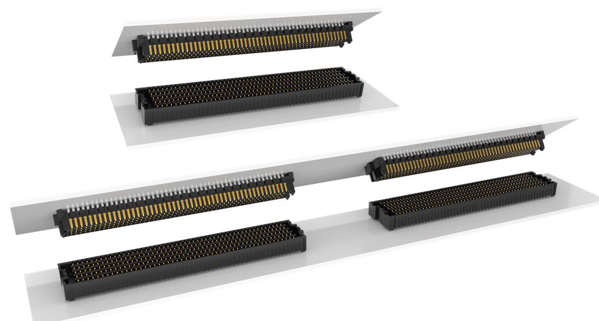
However, the addition of more mated connector sets onto the same mother-mezzanine card in any direction and at any distance will introduce several tolerances which will stack (Figure 2, bottom). These tolerances are unique to the PCB fab shop, the electronic manufacturing service, and the properties of the materials used in the PCBs.
To clarify the problem, consider a multiple mezzanine connector system (Figure 2).
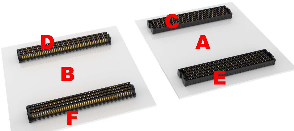
This assembly comprises six components or more: the motherboard (A), a mezzanine card (B), female connector #1, (C), which mates to male connector #1 (D), and female connector #2 (E), which mates to male connector #2 (F).
If mezzanine connectors and sufficiently rigid PCBs were fabricated, processed and assembled to exact nominal conditions, then an infinite number of connectors could be successfully deployed between two PCBs. In reality, variability within tolerance and material properties become the limiting or determining factors. In the case of Figure 1, designers need to consider and account for the tolerances of all components, including the often-neglected but relevant tolerances of the two PCBs, (A) and (B).
How to address the problem of PCB-connector alignment
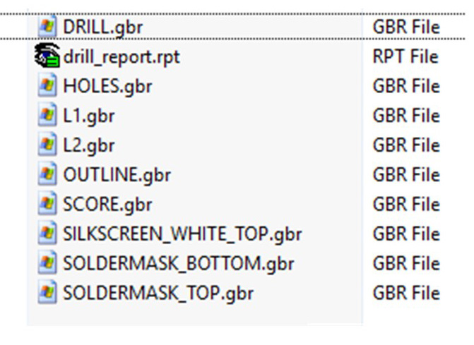
Some PCB purchases are controlled only by the specifications embedded in the Gerber packet (Figure 3). It is possible to build PCBs from these packets without any consideration for mechanical tolerances.
For multiple connector applications, separate mechanical drawings must accompany this packet which dictate artwork, drilling and routing tolerances.
It's at this point that the designer needs to do two things to help ensure a successful outcome. The first is to understand what to expect from the PCB supplier and the connector supplier in order to ensure alignment. The second is to be sure to have performed a system-level tolerance study to determine the connector misalignment generated by their design.
Referring back to the multi-connector mezzanine card system of Figure 2, A through F, a connector supplier can only control the tolerances of the connectors. A good supplier will meet or exceed published performance specifications, make PCB tolerance and processing recommendations, and even provide referrals for PCB suppliers and equipment recommendations, as needed.
The system or product designers should refer to the connector footprint and product specifications. The misalignment specifications contained in these documents should be compared to the results of the system-level tolerance study to help ensure the successful use of multiple connectors between the same card.
The connector system should function properly as long as the initial and final angular and linear misalignments are not exceeded. These misalignment values are calculated by taking into consideration factors such as insulator interference, beam deflection, and contact wipe. Exceeding the misalignment values could result in open or damaged circuits and/or insulators.
While designers usually have all of the necessary information at their fingertips with regard to their design, component tolerances, equipment, and manufacturing capabilities, it's important to be able to reach out to a connector manufacturer for more specific guidance and verification of misalignment tolerance stacks.
Alignment pins not suited to multiple-connector applications
Some connector manufacturers offer optional alignment pins, usually located on opposite sides of the bottom of the connector (Figure 4).

These pins assist in hand placement and can be used to polarize the connector to the PCB, and for single connector applications they do not contribute to the overall tolerance stack.
For multiple connector applications, however, alignment pins are not recommended as they contribute to the overall tolerance stack. If polarization on the PCB is still desired, a better option is to drill over-sized holes in the PCB and machine place the connectors.
Likewise, the use of fixtures or dowels to assist in connector placement is not recommended. These methodologies often rely on a drilled hole in the PCB relative to the artwork, but the positional tolerance of this hole is typically poor, which reduces the overall precision of final connector placement, relative to one another.
A better approach for multiple connector applications is to datum all solder pads from position A1 in solder pad array A, then look to precision-place the connectors on the pads prior to reflow.
Securing PCBs with jack screws
Some particularly rugged applications may require the use of jack screws to secure the two PCBs. In such instances, the screws should be placed as closely as possible to the connector system (Figure 5).
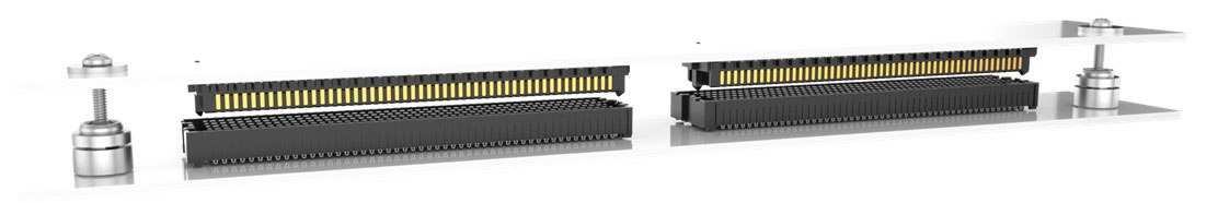
Placing them close will localize stress to the vicinity of the connector and decrease the unsupported PCB span. Increased spans will induce bending stresses in the PCB that could have detrimental effect on other components, particularly those that are surface mounted.
Another source of connector-derived PCB stress is loading, where a significant number of inputs and outputs (I/Os) can generate extremely large mating/unmating forces. These forces can cause excessive deflections in the PCB to the point that additional stiffeners are required to support the PCBs. It's important to always confirm connector mating and un-mating forces, as found in the product qualification test reports (Figure 6).

Conclusion
While miniaturization trends have made it more challenging, it is still possible to use multiple connector sets on two PCBs, using design best practices. These include performing a system tolerance study to determine the connector misalignment, following the connector provider's recommended footprint and stencil design recommendations, and machine placing components.
It's also advisable to engage closely with connector providers early in the design process as they can advise on types of connectors and placement, as well as provide counsel on how to minimize overall PCB and connector stress to help ensure a successful design.


